The global semiconductor industry is undergoing a fundamental recalibration, transitioning from a decades-long focus on concentrated efficiency toward a new paradigm of distributed resilience. Within this structural shift, the Memorandum of Understanding (MoU) signed on May 16, 2026, between Tata Electronics and ASML represents a definitive pivot in India’s industrial and geopolitical trajectory. This partnership, centered on the establishment of India’s first commercial 300 mm (12-inch) semiconductor fabrication plant in Dholera, Gujarat, is not merely a commercial transaction for high-tech equipment; it is the technical and diplomatic cornerstone of the India Semiconductor Mission (ISM) 2.0. By securing a long-term commitment from ASML, the world’s leading supplier of photolithography systems, India is addressing the primary technical bottleneck that has historically precluded its entry into front-end semiconductor manufacturing.
The broader context of this agreement is defined by the elevation of the India-Netherlands relationship to a “Strategic Partnership” during the visit of Prime Minister Narendra Modi to The Hague. This diplomatic framework provides the necessary scaffolding for high-stakes capital investments, aligning India’s massive domestic market and talent pool with the Netherlands’ specialized expertise in lithography and maritime logistics. As global supply chains face increasing volatility in the Taiwan Strait and across traditional manufacturing hubs, the Tata-ASML collaboration positions India as a “trusted geography” capable of supporting the “workhorse” chips that power the global automotive, telecommunications, and industrial sectors.
The Geopolitical Scaffolding: The India-Netherlands Strategic Alignment
The formalization of the Tata-ASML partnership occurred within a larger diplomatic theater, as the leaders of India and the Netherlands adopted the “Roadmap of India-Netherlands Strategic Partnership (2026-2030)”. This roadmap is a multi-dimensional blueprint for cooperation in sectors deemed critical for future economic security: semiconductors, green hydrogen, and advanced maritime logistics. The choice of the Netherlands as a primary technology partner reflects its role as a global innovation hub and the “Gateway to Europe,” anchored by the Port of Rotterdam.
| Pillar of the Strategic Roadmap (2026-2030) | Specific Objectives | Institutional Mechanisms |
| Technology & Innovation |
Cooperation in semiconductors, AI, quantum systems, and photonics. |
Joint Working Group on Emerging Technologies. |
| Economic & Trade |
Strengthening the India-EU FTA and increasing bilateral trade through logistics hubs. |
Overarching Joint Trade and Investment Committee (JTIC). |
| Energy Transition |
Launching the Green Hydrogen roadmap and accelerating renewable energy adoption. |
Joint Working Group on Renewable Energy. |
| Human Capital |
Establishing the “Brain Bridge” between universities and facilitating talent mobility. |
MoU on Mobility and Migration. |
| Maritime & Logistics |
Developing a “Green and Digital Sea Corridor” and modernizing port infrastructure. |
Joint Working Group on Maritime Cooperation. |
The joint statement issued by Prime Minister Modi and Dutch Prime Minister Rob Jetten emphasizes “resilient and trusted supply chains” as a cornerstone of the bilateral relationship. This alignment is a direct response to the “decade of crises” identified by the Indian leadership, which includes the supply chain shocks of the COVID-19 pandemic and the geopolitical tensions in West Asia and Eastern Europe. By designating India as a “symbol of scale and stability,” the Dutch government is essentially endorsing India’s capacity to host the complex, multi-tiered ecosystem required for semiconductor manufacturing.
The strategic importance of this endorsement cannot be overstated. ASML’s dominance in lithography means that almost every cutting-edge chip in the world is manufactured using their technology. Consequently, ASML’s willingness to partner with Tata Electronics serves as a “global signaling mechanism,” indicating that India has reached the requisite level of policy stability and infrastructure readiness to enter the front-end of the semiconductor value chain.
Technical Foundations: The Dholera Fab and Lithography Integration
The Dholera fab, representing an investment of approximately $11 billion (₹91,000 crore), is designed to produce 50,000 wafer starts per month (WSPM) using 300 mm silicon wafers. The partnership with ASML provides the facility with its most critical component: the “holistic suite” of advanced lithography tools. Lithography is the most capital-intensive and technologically demanding phase of semiconductor manufacturing, acting as a highly specialized printing press that uses light to etch microscopic circuit patterns onto wafers.
The Mechanics of Holistic Lithography
ASML’s involvement goes beyond the mere delivery of hardware. Their “holistic” approach integrates several layers of technology to ensure high yield and manufacturing excellence:
-
Lithography Systems: Deployment of advanced DUV (Deep Ultraviolet) systems suitable for mature nodes, which form the core of the Dholera facility’s production capacity.
-
Computational Lithography: Software solutions that optimize the mask designs and light patterns to minimize errors at the microscopic scale.
-
Metrology and Inspection: E-beam and optical inspection systems that measure pattern quality in real-time, allowing for immediate process adjustments to maintain high yields.
The facility is being developed in collaboration with Taiwan’s Powerchip Semiconductor Manufacturing Corporation (PSMC), which provides the foundational process technology. The addition of ASML as a strategic equipment partner ensures that the fab has the necessary technical support to “ramp up” production efficiently, reducing the learning curve often associated with new facilities.
Strategic Process Node Selection: Why 28nm to 110nm?
While the global media often focuses on the “bleeding-edge” 2nm or 3nm nodes used in top-tier smartphone processors, India’s strategic focus on the 28nm to 110nm range is a calculated and commercially prudent entry point. These “mature nodes” are the workhorses of the global semiconductor market.
| Technology Node | Primary Market Applications | Economic Significance |
| 28nm |
Automotive processors, 5G base stations, high-end IoT, and AI edge devices. |
The “sweet spot” for performance vs. cost; remains commercially critical for decades. |
| 40nm – 65nm |
Power management ICs, microcontrollers for industrial machinery, and consumer electronics. |
High-volume demand with stable production processes and manageable capital expenditure. |
| 90nm – 110nm |
Analog sensors, automotive engine control units (ECUs), and medical devices. |
Foundational components for the automotive and defense sectors where reliability is paramount. |
By targeting these nodes, Tata Electronics is addressing the segments where demand is most stable and supply chain shortages are most acute. For example, a modern electric vehicle (EV) requires hundreds of mature-node chips for everything from battery management to infotainment systems. Securing domestic production of these chips is a prerequisite for India’s ambition to become a global leader in EV manufacturing and electronics export.
Human Capital: The “Brain Bridge” and Workforce Training
The single greatest risk to the long-term success of India’s semiconductor mission is the potential shortage of specialized talent. The Tata-ASML MoU explicitly addresses this by committing both companies to the development of a domestic talent pipeline. This effort is bolstered by the “Brain Bridge” initiative, a landmark academic-industrial collaboration.
Academic Synergy and Research Infrastructure
The Brain Bridge is anchored by a Memorandum of Cooperation involving two Dutch universities—Eindhoven University of Technology and the University of Twente—and six of India’s premier technical institutes. This program is uniquely supported by a consortium of industry leaders, including ASML, NXP, Tata, and CG Semi.
| Indian Institute | Key Role in the Brain Bridge | Dutch Partner |
| IISc Bangalore |
Advanced materials research and semiconductor physics. |
Eindhoven University of Technology |
| IIT Delhi |
Centre of Excellence on Water and system-on-chip (SoC) design. |
University of Twente |
| IIT Bombay |
Nanotechnology and fabrication process optimization. |
Eindhoven / Twente |
| IIT Madras |
Digital systems and power electronics for automotive applications. |
Eindhoven University of Technology |
| IIT Guwahati |
Semiconductor materials for the Morigaon, Assam ecosystem. |
University of Twente |
| IIT Gandhinagar |
Specialized training in lithography-intensive skillsets. |
Eindhoven / Twente |
The collaboration focuses on creating a “seamless talent pipeline,” where Indian students can engage in research that is directly applicable to the equipment used by ASML and the processes managed by Tata Electronics. Furthermore, ASML has already established a network of training centers globally, such as the 56,000-square-foot facility in Arizona, which serves as a potential blueprint for a specialized “ASML Technical Academy” in India. These centers offer immersive training in cleanroom environments, ensuring that engineers are proficient in the maintenance and operation of complex lithography modules before they even step onto the fab floor.
Social Impact: Women in the High-Tech Workforce
The semiconductor sector in India is also emerging as a catalyst for gender-inclusive industrialization. Tata Electronics has demonstrated a consistent commitment to employing large numbers of women in its workforce. In its existing electronics facilities in Tamil Nadu and Karnataka, female participation has reached nearly 80-90%.
The “campus model” pioneered by Tata Electronics—which provides safe accommodation, transport, and a secure environment—is identified by experts as a critical factor in this success. As the Dholera fab and the Morigaon, Assam assembly unit ramp up, the company plans to replicate this model, providing significant economic opportunities for women in regions where high-tech employment was previously unavailable.
Ecosystem Expansion: The Morigaon OSAT and Dholera Smart City
The Dholera fab is the crown jewel of India’s semiconductor strategy, but it does not exist in isolation. The India Semiconductor Mission is fostering a “hub-and-spoke” model that connects fabrication with assembly, testing, and urban infrastructure.
The Mega OSAT Facility in Morigaon, Assam
While Dholera handles the “front-end” manufacturing (etching designs onto wafers), Tata Electronics is also building a massive “back-end” facility in Jagiroad, Morigaon, Assam. This greenfield project represents an investment of over ₹27,000 crore ($3 billion+) and is designed for high-volume Outsourced Semiconductor Assembly and Test (OSAT).
The Assam facility is engineered to produce billions of chips per year, utilizing state-of-the-art AI-enabled manufacturing processes. Its portfolio includes several critical packaging technologies:
-
Wire Bond: Using fine wires (gold, aluminum, or copper) to establish electrical links, ensuring reliable power and signal transfer.
-
Integrated System Packaging (ISP): A transformative technology that combines diverse components—microprocessors, sensors, and power management—into a single, compact package for AI and mobile devices.
-
Flip Chip: A high-density interconnection technique using solder bumps that minimizes signal path length and enhances thermal performance, which is vital for high-performance computing.
By establishing the Morigaon plant, Tata Electronics is creating a vertically integrated domestic supply chain. This reduces India’s reliance on East Asian hubs for the final stages of production and enhances the “speed to market” for domestic electronics manufacturers.
Dholera Smart City: Infrastructure for the Future
The Dholera Special Investment Region is more than just a site for a factory; it is being developed as India’s first greenfield “Smart City” of this magnitude. Projected to create over eight lakh (800,000) new jobs, Dholera is designed to be “digital-first,” featuring an integrated command center for security and emergency services. The city’s urban framework includes dedicated housing for all income levels, modern healthcare facilities, and cultural centers, which are essential for attracting the international and domestic experts required to operate a world-class fab.
| Feature of Dholera Smart City | Strategic Significance |
| Integrated Command Center |
Provides 24/7 security monitoring and emergency response for residents and industry. |
| Greenfield Planning |
Allows for the integration of digital infrastructure and sustainable water management from day one. |
| Industrial-Urban Balance |
Prevents the congestion and pollution typically associated with rapid industrial hubs. |
| Strategic Location |
Connectivity to major ports and the Delhi-Mumbai Industrial Corridor (DMIC). |
India Semiconductor Mission 2.0: Policy and Market Projections
The India Semiconductor Mission (ISM) has evolved from a series of policy incentives (ISM 1.0) into a tangible network of operational units (ISM 2.0). The Union Budget 2026-27 provided a significant boost to this mission, with a total financial outlay of ₹8,000 crore for the development of the semiconductor and display manufacturing ecosystem.
Roadmap to Technological Sovereignty
The government’s roadmap is focused on deepening domestic capabilities across the entire value chain:
-
By 2029: India aims to design and manufacture the chips required for 70-75% of its domestic applications.
-
By 2030: The Indian semiconductor market is projected to reach $100-$110 billion.
-
By 2035: India envisions being among the top semiconductor nations globally, with a defined roadmap to achieve 3nm and 2nm technology nodes.
This ambitious timeline is supported by a strategy of “trusted geography”. As global firms look for alternatives to the concentrated production hubs in Northeast Asia—the “China +1” strategy—India’s combination of democratic values, a massive talent pool, and significant government subsidies makes it a compelling destination for diversification.
Comparative Market Outlook
While India is starting behind established giants like TSMC (Taiwan) and Samsung (South Korea), the current path mirrors the early industrialization stages of those very nations in the 1970s and 1980s. By focusing on mature nodes (28nm-110nm), India is entering a market with high barriers to entry but also high resilience and long-term demand stability.
| Metric | India’s Target (2030-2035) | Global Context (2026) |
| Front-end Fabs |
Multiple commercial 300mm fabs (Dholera being the first). |
Dominated by TSMC, Samsung, Intel. |
| Packaging (OSAT) |
Billions of chips per year capacity (Morigaon, Vemgal). |
Majority of capacity currently in Taiwan and China. |
| Design Ecosystem |
Capability for 70%+ of domestic applications. |
India already hosts design centers for all major global chipmakers. |
| Lithography Access |
Strategic Partnership with ASML for holistic solutions. |
ASML holds a near-monopoly on critical equipment. |
Strategic Risk Assessment and Competitive Dynamics
Despite the significant momentum, the success of the Tata-ASML partnership and the broader ISM faces several challenges that require proactive management.
Geopolitical and Export Control Risks
The reliance on ASML is a critical dependency. As the sole provider of advanced lithography, ASML is often at the center of US-China trade disputes. India must maintain its status as a “neutral and trusted” partner to ensure that its access to high-tech equipment is not hindered by future export controls. The elevation of the India-Netherlands relationship to a Strategic Partnership is a calculated move to secure this technology pipeline.
Execution and Infrastructure Challenges
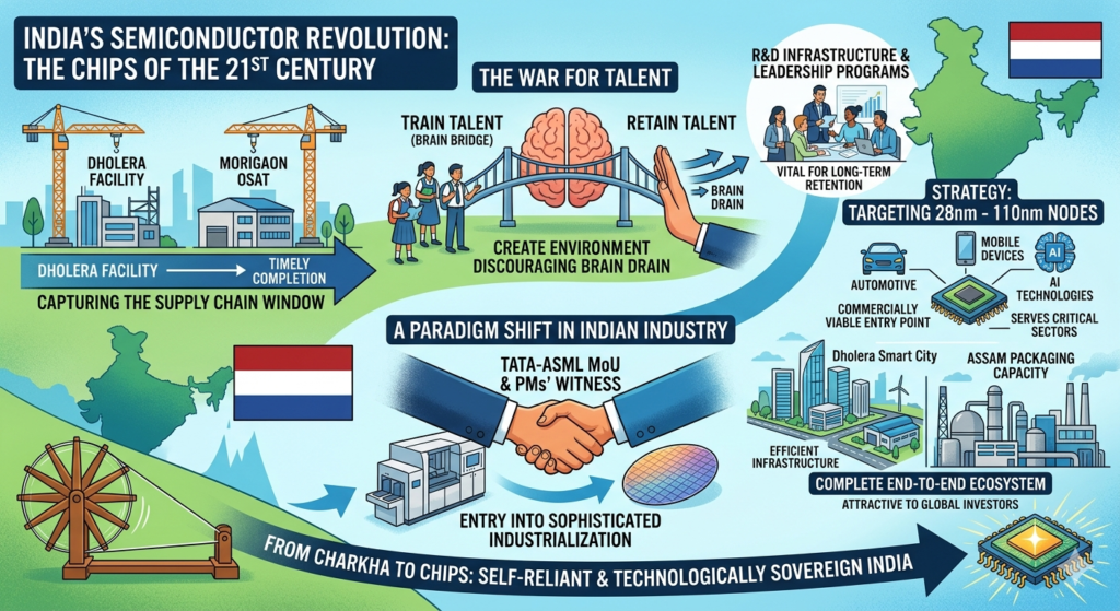
Operating a 300 mm fab requires massive, uninterrupted supplies of ultra-pure water, specialized industrial gases, and stable electricity. The Dholera project’s success depends on the rapid completion of these supporting utilities. The partnership with Dutch water management experts and the establishment of a “Green and Digital Sea Corridor” are intended to address these logistical needs. Furthermore, the construction timelines for the Dholera facility and the Morigaon OSAT must be strictly met to capture the current window of global supply chain diversification.
The “War for Talent”
While the Brain Bridge initiative is a strong starting point, the global competition for semiconductor engineers is fierce. India must not only train talent but also create an environment that discourages the “brain drain” to established hubs in the US or Europe. The commitment of Tata Electronics to building R&D infrastructure and providing leadership opportunities through early career programs is vital for long-term retention.
Conclusion: A Paradigm Shift in Indian Industry
The signing of the Tata-ASML MoU, witnessed by the Prime Ministers of India and the Netherlands, signifies more than the launch of a factory; it marks India’s entry into the most sophisticated tier of global industrialization. By securing the “beating heart” of the semiconductor fab—the lithography machines from ASML—and aligning this with a comprehensive workforce development strategy, Tata Electronics is laying the foundation for a self-reliant and technologically sovereign India.
The strategy of targeting the 28nm to 110nm nodes provides a commercially viable entry point that serves the world’s most critical sectors: automotive, mobile, and AI. When combined with the massive assembly and packaging capacity being built in Assam and the urban-industrial framework of the Dholera Smart City, India is creating a complete, end-to-end ecosystem that is attractive to global investors and resilient to geopolitical shocks.
As Prime Minister Modi noted during his visit to The Hague, the strengthening strategic partnership between India and the Netherlands is giving a “new impetus” to the business relationship. The transition “from charkha to chips” is now well underway, positioning India as a vital, trusted, and innovative hub in the global silicon landscape of the 21st century.